
|

|
|
|
|
|
Wire r = reg(a);
This will build a bank of flip flops (wide enough for the bits of
a) and connect a to its inputs and r to its
outputs. It will also cause the creation of a global clock wire (if
none exists yet in the design) and
wires it up to the implicit clock wire on each of the flip flops.
For simulation purposes, a clock generator will also be created which will
alternately drive this clock wire low and high.
The created clock wire and its behavior will be visible in the schematic and waveform viewers.
All Logic methods which create synchronous circuitry such as reg() have versions which contain an explicit clock wire and those (like above) for which the clock wire is implicit. All synchronous primitive cells also have implicit- and explicit-clock constructor versions. When using the implicit versions, JHDL will create and wire up the default global clock as needed.
Thus, it is recommended that, unless you have a specific need, that you use default clocking for your designs. This is accomplished by simply calling only the versions of primitive constructors and Logic methods which contain no explicit clock wire. It is the simplest approach and will result in the fastest simulations of your circuits.
import byucc.jhdl.base.*;
import byucc.jhdl.Logic.*;

public class add_ex1 extends Logic {
  public static CellInterface[] cell_interface = {
    in("reset",1),
    out("count",4),
  };

  public add_ex1(Node parent,
                   Wire reset,
		   Wire count) {
    super(parent);

    connect("reset",reset);
    connect("count",count);

    reg_o(mux(add(count,constant(4,1)),constant(4,0),reset),count);
  }
}
This is a simple counter with a reset and is constructed from a register, a mux, and an AND gate. The register requires a clock and JHDL adds the clock wire appropriately. The clock wire can be seen in the following schematic:
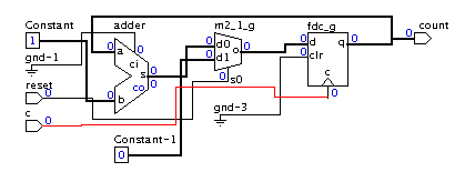
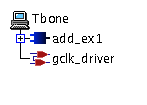
The clock wire is driven by a simulation model of a clockDriver and that clock driver can be seen here in the tree view in cvt.
Every clock driver in the system (here there is only gclk_driver) has a clock schedule that represents pattern of bits which will be repeated on the clock wires. A clock schedule is applied during across the length of a cycle. Each entry in the clock schedule is a step in the cycle. So for the default clock, the schedule is "01" meaning that in the first phase of a cycle's simulation the default clock is low and for the second phase the default clock is high.
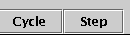
Step and cycle commands are used to tell the simulator to execute the simulation. A step executes a single element of the clock schedule. Cycle executes to the end of the current cycle.
The step and cycle buttons are located on the lower left side of the cvt window:
The default clock and its schedule can be seen in the following waves view:
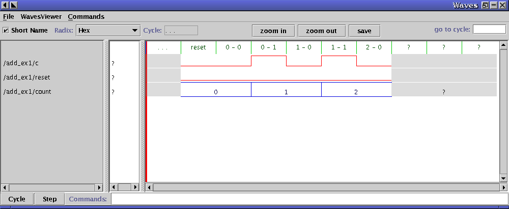
The top wire represents the clock schedule 01 for the default clock driver. In cycle 0 step 0 (e.g. 0 - 0) the clock driver drives 0. During the next clock step (0 - 1) the clock driver is driving a 1.
However, there will be times when a design must contain more than one
clock. A typical example would be an FPGA board where the memory
subsystem is clocked at a different rate than the FPGA fabric. In
this case, the user cannot use default clocking but must define the
various clocks in the system, their simulation schedules, and
explicitly state which synchronous elements are wired to which
clocks. This is described in complete detail later in this user's
manual in User-Defined Clocking and
Multi-Clocking.
| | JHDL Home Page | Configurable Computing Lab | Prev (Module Generators) | Next (Circuit Verification) | |
![]()
JHDL 0.3.45
Copyright (c) 1998-2003 Brigham Young University. All rights reserved.
Last updated on 11 May 2006