
|

|
|
|
|
|
"Placement" involves grouping the primitive logic blocks on an FPGA. For example, placement in the Xilinx XC4000 architecture involves grouping the previously mapped LUTs and flip-flops into the appropriate CLBs and grouping the CLBs together on the FPGA. "Relative placement" refers to placing LUTs, flip-flops and CLBs relative to each other, and "absolute placement" refers to placing LUTs, flip-flops and CLBs at absolute locations of the FPGA.
Mapping and Placement will always be done during the back-end compilation step by automated map and PAR tools. However, if a user wishes to customize or optimize how circuitry is mapped or placed together, manual mapping and placement can be done during the design entry stage. For the rest of this manual, mapping and placement refer to the manual mapping and relative placement done during the design entry stage of circuit design.
     Wire out = and( a, b );
     map(a, b, out);
     place( out, 2, 5 );
The first line creates an AND gate with a and b as inputs and out as the output. The second line maps a and b as inputs to a 4-LUT with out as the output. The last line places the the AND gate at the relative location (2,5). Note that in this example, the output wire was the object being placed. In JHDL, calling place() on a reference to the cell or on the output wire of the cell have the same effect--both result in the placement of the cell that drives the output wire.
We will give a more detailed explanation of the map() and place() calls later in the tutorial.
     Wire out = or( and(a,b), and(a,ci), and(b,ci) );
     map( a, b, ci, out );
this implies mapping the function of the three AND gates and one OR gate into a single LUT in XC4000. The map() call currently accepts from 2 to 9 input parameters, and optionally accepts a String that gives target-specific constraints to the platform-specific TechMapper. See the documentation for your specific FPGA architecture for a list of possible constraints.
It is important to note that the Logic API defines absolutely nothing about the exact implementation of the map() call, beyond what has been specified here. The optional String arguments accepted by map() are specifically "defined to be undefined" in the Logic class! They receive no interpretation in the Logic class, and are passed straight to the TechMapper for platform-specific interpretation.
Technology mapping can be done explicitly by instantiating individual primitives. In the case of a full-adder in XC4000 we would write.
     or_o(and(a,b), and(a, ci), and(b, ci), sum);
     xor_o(a, b, ci, co);
     fmap f1 = new fmap(this, a, b, ci, sum);
     fmap f2 = new fmap(this, a, b, ci, co );
However, this limits technology independence since fmaps are specific to Xilinx Parts. The same thing can be achieved by targeting the XC4000TechMapper and implementing the fmaps through the Logic map() method. Using the Logic map() call still requires a knowledge of how logic is packed together into the basic FPGA elements. For example, the adder would be mapped to 2 LUTs in Xilinx XC4000. With this knowledge, the Logic methods look like this:
     or_o(and(a,b), and(a, ci), and(b, ci), sum);
     xor_o(a, b, ci, co);
     map(a, b, ci, sum);
     map(a, b, ci, co);
The above map methods will pass all the associated information to the TechMapper.
NOTE: While some error checking is done in the techmapper, users are advised to learn the restrictions of a technology before attempting to use the map method. For example, if you are trying to pack the logic into a 4-LUT in Xilinx XC4000, it doesn't make sense to use a map() call with nine input wires unless it is clear to the TechMapper how the nine inputs can be distributed among the various LUTs. For example, the following code would be valid in XC4000 since the 4-input and-gate and xor-gate can be mapped to the F-LUT and G-LUT, while the 3-input or-gate can be mapped to the H-LUT.
     Wire out = reg( or( a, and(b,c,d,e), xor( and(f,g), or(h,i) ));
     map( a,b,c,d,e,f,g,h,i, out );
     Wire a = wire(5);
     Wire b = wire(5);
     Wire ci = wire(5);
     Wire co = wire(5);
     Wire sum = wire(5);
     or_o(and(a,b), and(a, ci), and(b, ci), sum);
     xor_o(a, b, ci, co);
     map(a, b, ci, sum);
     map(a, b, ci, co);
Each map method in this case would create 5 fmaps for the XC4000 architecture.
For most technologies, the wire widths in a map() call must be any combination of the atomic width or a single "generic" width. For example, in the Xilinx XC4000 architecture the following set of wire widths would be valid: { 1, 8, 8, 1, 8 }. On the other hand, the following set would be invalid, because there is more than one "generic" width: { 1, 8, 4, 1, 8 }. (Basically, in this case "generic" means anything other than 1-bit).
Logic Map methods return the new mapping cell or the driver of the output wire for future use in placement or layout manipulation.
Placement "hints", or properties, may be specified in many different ways. The most basic method, which allows users very fine-grained control without JHDL intervention, is to use the addProperty() method. To place the 1-bit full adder of the previous example in XC4000, we could use the following code:
    or_o(and(a,b), and(a, ci), and(b, ci), sum);
    xor_o(a, b, ci, co);
    map(a, b, ci, sum).addProperty("RLOC", "R0C0.F");
    map(a, b, ci, co).addProperty("RLOC", "R0C0.G");
This will append the property string "RLOC=R0C0.F" onto the fmap returned by the map method for the add logic, and append the property string "RLOC=R0C0.G" onto the fmap for the carry logic.
The place() method in Logic is designed to be a convenient way to append placement hints onto a cell. Placement hints can be added directly to cells without using an RLOC string by doing the following:
    place(Cell Sum, "R0C0.F");
    place(Cell Carry, "R0C0.G");
The place() calls simply attach an RLOC property with the given value to the specified Cells.
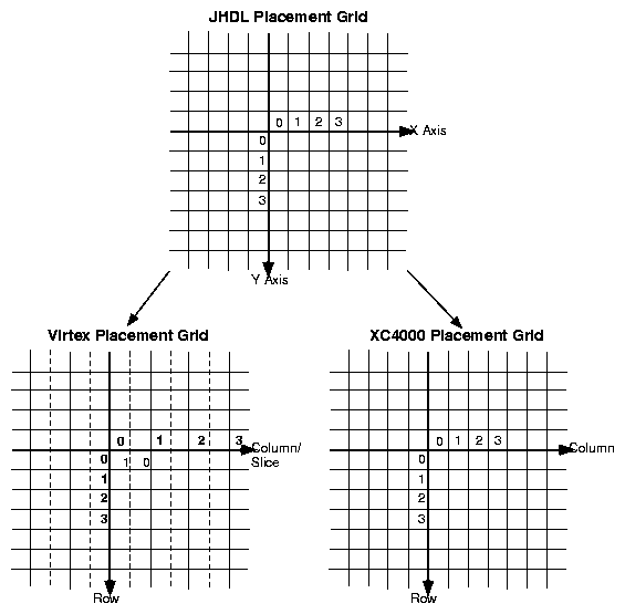
In order to preserve some notion of technology independence for placement, a generic grid of X and Y coordinates is used in Logic and interpreted by each TechMapper. At netlist time these X and Y coordinates, together with their hints, are converted into properties like the RLOCs for XC4000 and attached to the appropriate cells. The JHDL placement grid has Logic calculate some of the placement hints before Technology Mapping and determine if a given cell can be placed by the TechMapper. The JHDL placement grid also allows the use of ints instead of strings in the place() calls, which simplifies the programming process. For example, using the JHDL grid the place() calls from above for XC4000 would be:
    place(Cell Sum, 0, 0, ".F");
    place(Cell Carry, 0, 0, ".G");
The conversion from a JHDL placement grid to XC4000 and Virtex is illustrated below:
Placement in this fashion can be done in the following way for the Full-Adder example in XC4000.
     or_o(and(a,b), and(a, ci), and(b, ci), sum);
     xor_o(a, b, ci, co);
     map(a, b, ci, sum);
     place(sum, 0, 0, ".F");
     map(a, b, ci, co);
     place(co, 0, 0, ".G");
This code will place the sum logic at X=0, Y=0 with a ".F" string property that will be passed to the TechMapper of choice and interpreted there. The same will be true of the carry logic except it will have the ".G" string. Since the TechMapper is for XC4000, it interprets the strings to put the logic at location (0,0) in the F-LUT and G-LUT, respectively.
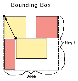
Relational cell placement is done by using width, height, and location information about cells to compute a new placement location. This information ( Width, Height, X, Y ) is stored in each cell and can be accessed through the following cell methods:
     getWidth()
     getHeight()
     getX()
     getY()
By themselves, these methods do not accomplish much, but convenience methods such as the Logic place() call use them to make placement much easier. The basic format for relational cell placement is:
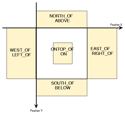
place(Cell curr, Directive dir, Cell prev);
Just as if reading a sentence, this method would place the current cell
in the direction dir from a previously placed cell. For example, absolute placement
of a registered adder might look something like this:
    Wire sum = add(a,b);
    Wire out = reg(sum);
    place(sum, 0, 0);
    place(out, 1, 0);
However, the same placement could be achieved with relational
placement in the following way:
    Wire sum = add(a,b);
    Wire out = reg(sum);
    place(out, RIGHT_OF, sum);
Recall that either a reference to the cell or the output wire of the cell can be used in the place() call to place the cell. Notice that the relational placement does not require knowledge about the width of the register or the adder. These methods can be simply read as "place the register to the right of the adder". The relational methods in Logic will decide where the register should be placed based on the specified direction.
|
 |
When a relational placement method like the one below is used, several steps are followed to place Cell1.
place(Cell1, Directive, Cell2);
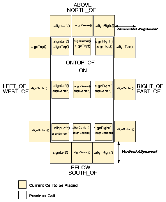
To show how this is done, consider the alignment methods provided by the Directive class:
place( CellA, RIGHT_OF.alignTop(), CellB);
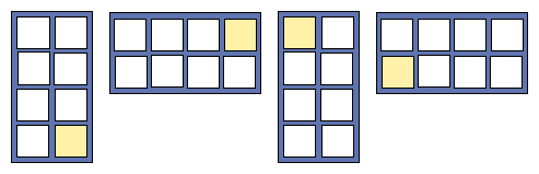
The above method would thus read "place CellA to the right of CellB such that top edges are aligned". If Directives are used without these alignment methods, then the default will be to align left edges, top edges, or both. The following figure illustrates the positioning of the alignment directives:
 |
     Cell multiplier = new arrayMult(this, OperandA, OperandB, Clk_en, Product, signed, fully_pipelined);
     place(multiplier, 0, 0);

     Cell accumulator = new accum(this, Product, Clear, Add, Clk_en, Total);
     place(accumulator, RIGHT_OF, multiplier);
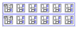
The result would look something like this in the XC4000 Layout viewer:
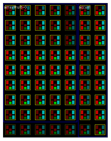
The blue lines in the above figure indicate the bounding boxes and the text indicates the names of the placed cells. As expected, the accumulator was placed to the right of the array multiplier.
Currently, 3 transformations exist: scale, rotate, and translate . They are all methods in the logic class and will accept either cells or output wires as their parameters.
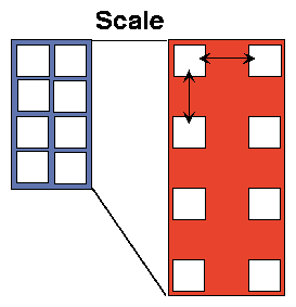
The scale method is designed to stretch a cell's layout by xFact in the x direction and yFact in the y direction. It works by recursively moving children cells to the new position x = x*xFact, y = y*yFact and then recomputing the cell's bounding box. This scaling of the layout can only be done before a cell is placed.
The figures below show the following (in-use registers are marked by blue squares):
LIMITATIONS
Currently, the scale method only accepts integer factors. Great care should also be taken to ensure that asymmetric features of the FPGA are not scaled, as this will cause an error in the back-end compilation.
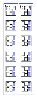
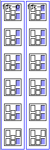
The rotate method rotates a Cell's layout by deg degrees in a counter-clockwise direction. It is implemented by recursively moving children to a new position, and then recomputing each cell's bounding box. Again, the rotate method is only valid on a cell that has not yet been placed and has many of the same limitations as scale.
ROTATION by 0, 90, 180, 270 degrees
Wire d = wire(11);
Wire q = wire(11);
Cell regbank = new regBank(this, d, q);
rotate(regbank, 90);
place(regbank, 0, 0);
The result would look like this in XC4000 (in-use registers are marked by blue squares):
![]()
The translate method allows users to move a Cell by dx and dy from it current position. It has the exact same effect as using place(x+dx, y+dy); where x and y are the cell's current placement position. Unlike scale and rotate, translate can only be used after a cell is placed.
new Mod1(this, in1, in2, out);
Wire delay = reg(out);
place(Mod1, 0, 0);
place(delay, RIGHT_OF.alignBottom(), out);
translate(delay, -1, -1);
This is the most verbose method for relational port placement. It directs
Logic to place currcell in the direction of
dir from
prevcell,
aligning
inWire and outWire.
The steps to doing this relational port placement are as follows.
To eliminate most of the verbosity of the relational port placement method, relational port placement can be done through the relational cell placement methods. This is done by using alignment methods on the Directive which specify the wire to align the two cells with.
To illustrate consider the placement of a registered adder.
Wire sum = add(a,b);
Wire out = reg(sum);
place(out, ONTOP_OF.align(sum), sum);
The above code segment would place the adder at X=0, Y=0 and then place the register in the same location as the adder so that the sum wire fed directly out of the adder and into the register.
| | JHDL Home Page | Configurable Computing Lab | Prev (Importing Designs) | Next (Tri-state) | |
![]()
JHDL 0.3.45
Copyright (c) 1998-2003 Brigham Young University. All rights reserved.
Last updated on 11 May 2006