
|

|
|
|
|
|
The first circuit we will describe is a full-adder. We will step through this in detail, emphasizing important points. Here is the code: (FullAdder.java )
// Import the base libraries for JHDL design
import byucc.jhdl.base.*;
import byucc.jhdl.Logic.*;

// Our FullAdder is a Java class.  Begin the class declaration here
public class FullAdder extends Logic {

  // This is cell's interface (ports)
  public static CellInterface[] cell_interface = {
    in("a", 1),
    in("b", 1),
    in("cin", 1),
    out("sum", 1),
    out("cout", 1)
  };

  // This is the constructor - it gets called when a new FullAdder is desired
  public FullAdder(Node parent, Wire a, Wire b,
		   Wire cin, Wire sum, Wire cout) {

    // Since we extend Logic, always have to call its constructor as the first thing
    super(parent);


    // Connect the wires passed in as parameters to the constructor to
    // the ports from the CellInterface above.
    connect("a", a);
    connect("b", b);
    connect("cin", cin);
    connect("sum", sum);
    connect("cout", cout);

    // Build our logic as a collection of gates.
    or_o( and(a,b), and(a,cin), and(b,cin), cout ); /* cout is output */
    xor_o( a, b, cin, sum );                        /* sum is output */

  }
}
JHDL is a Java-based HDL, and so every circuit in JHDL is an object. Wires, logic gates, and other circuit building blocks are also objects. In order to be able to instantiate these JHDL building blocks, we must import their class files. The first lines in your circuit description should import the class files byucc.jhdl.base.* and byucc.jhdl.Logic.*.
      import byucc.jhdl.base.*;
      import byucc.jhdl.Logic.*;
With these class files available, we can now begin to describe our
circuit. Our circuit is an object, so we declare it as a class with:
public class FullAdder extends Logic {
By extending Logic we can have access to methods that will build the gates
in our circuit. For now, always have your circuits extend Logic.
These lines declare the ports on your circuit:
       public static CellInterface[] cell_interface = {
          in("a", 1),
          in("b", 1),
          in("cin", 1),
          out("sum", 1),
          out("cout", 1)
       };
Each circuit you build should have ports (unless you don't ever want to use it). Ports are used to connect wires to the circuit block when it is instantiated. These ports are described in the CellInterface. The static object cell_interface describes an array of these ports. Each port must be described by a direction, a name, and a width. For example:
in("a", 1)
describes an input port named "a" that is 1 bit wide. Output ports are described with out(name,width).
Having declared the interface to your circuit, you now must write a constructor for your circuit (all Java classes have constructors). The constructor is the method (subroutine) that gets called when your circuit gets built. Here is the beginning of the constructor:
      public FullAdder(Node parent, Wire a, Wire b,
                       Wire cin, Wire sum, Wire cout) {
It is a public subroutine. It takes six parameters. The first will tell it who its parent in the circuit hierarchy is. The next five are the wires that should be connected to its ports (a, b, cin, sum, and cout).
The next line:
super(parent);
is always required. Java programmers will know that this is calling the constructor of the class this circuit extended (Logic). Non-Java programmers need not worry - just always do this and don't ask a lot of questions (you needn't know why this is required).
Next, we must connect the wires that were passed into the constructor to the ports that were declared in the CellInterface above. This is done using these lines:
       connect("a", a);
       connect("b", b);
       connect("cin", cin);
       connect("sum", sum);
       connect("cout", cout);
Most cells are useful only if they perform a logic function on the inputs and pass the result to the outputs. Once wires are connected to the ports of the cell, the only thing left is to describe the logical function of the cell. This is done in the next two lines of our constructor:
       or_o( and(a,b), and(a,cin), and(b,cin), cout ); /* cout is output */
       xor_o( a, b, cin, sum ); /* sum is output */
Our cell's logic is described with calls to Logic methods and(), or_o(), and xor_o(). The first line above performs an or on the outputs of three 2-input and gates and returns the output to cout. The second line performs an xor on three inputs and puts the result on the output wire sum.
Note that the Logic class provides two types of methods to instantiate gates: gate() and gate_o(). For instance, we use and() calls inside the or_o() call. gate_o() and gate() differ only that the output wire is passed to gate_o(), whereas gate() returns a newly created output wire. It is important that we use the _o methods to connect logic to outputs. Otherwise our output wire pointer will be replaced with a new wire created by the gate() method and no logic will be connected to the output.
We're now done. The above circuit description is complete.
To review, the steps in the above code were the following:
Before continuing on with your JHDL desing, make sure that your development environment is properly set up. Running through a basic Java tutorial and properly setting your CLASSPATH should be sufficient to verify that your system is properly set up.
With your circuit description complete, you can now simulate your circuit using the JHDL Circuit Visualization Tool (CVT). First, let's compile your circuit. On a UNIX machine it is as simple as this:
javac FullAdder.java
This simply calls the Java compiler to compile your circuit. You are now ready to run. Type this to load your circuit in CVT:
java dtb FullAdder
This will start a new Dynamic Test Bench (dtb), which will load your circuit and create a new CVT system to view it. The resulting CVT window should look like this:

Once you have loaded a circuit you will see a tree appear in the left hand pane of the CVT window. You can use this tree to traverse the hierarchy of the circuit. As you select cells, you will notice that the wire names, widths, type, and current value of their ports are displayed in the right hand pane of the CVT window. You will note that your circuit is the FullAdder icon. Click the plus sign to the left of it and you should see this:

What you see is that FullAdder contains some gates of various types.
Now, click on the FullAdder icon itself so that the name FullAdder is highlighted in color. From the Cell menu at the top of the window, select View Cell Schematic. (The shortcut methods are to either select the "FullAdder" icon and press "Ctl-S" or just double-click on the FullAdder icon.) A new window which contains a schematic of your adder should pop up like this:

Click on the Cycle in the main CVT window button. The circuit simulator program initializes and the values on the schematic are updated to reflect the current values of those wires in the simulator (currently everything is zero - not very interesting).
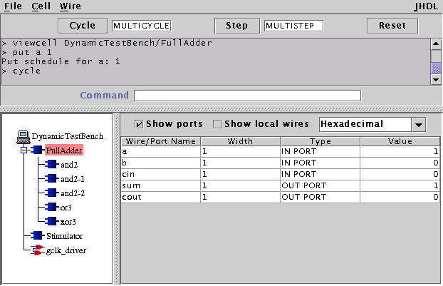
Click in the command box in the middle of the CVT window and type: put a 1. Then click the cycle button and the window looks like this:

As you can see, the value of a was updated in the schematic as well as the computed sum output value. You can use commands such as these to put values on any inputs and see the results.
Now, let's use the waveform viewer. Close the schematic window by selecting the Close command from the File menu. Back in the main CVT window, click on the FullAdder icon in the tree viewer so that its name in the TreeViewer is highlighted.
What you see is a representation of the ports on your FullAdder cell. The next column (Width) tells the port width, the next tells its direction, and the next its current value in the simulator. Click on the line of the table for port a then select the Watch wire command under the Wire menu. (The shortcut methods are to either select the a port and press "Ctl-W" or just double-click on the port in the table.) This causes the following window to appear:
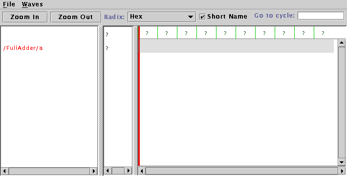
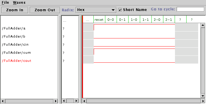
This is the waveform viewer window. Without closing this new window, go back and select the other wires in the wires table of the main CVT window and select the Watch wire command from the Wire menu. Then, click the cycle button 3 times and switch back to the waveform viewer window. You should get this:
As you can see, signal a is high and signal sum is high. Now, set b high by typing put b 1 in the command box in the main CVT window. Cycle once. Then, set cin high and cycle similarly. You should see something like this in the waveform viewer (you may need to click on the zoom in or zoom out button to get a similar view):
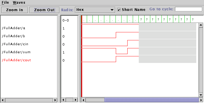
From the display it should be clear that the adder seems to be working. Now, close the waveform window and go back to the main CVT window.
Here is the console from this session:

You can continue to put values on wires from this window and continue to simulate.
netlist -insertpads t -f FullAdder.edn
This tells it to first automagically insert I/O drivers for the
top-level ports on your circuit (input ports get IBUF's, output ports
get OBUF's). It then tells it to generate EDIF and write that into the
file FullAdder.edn.
The n-bit adder circuit description is called NBitAdder.java. Notice that this cell also imports important classes, calls super(parent) in its constructor, and defines an interface. However, it has a number of new features over the previous example:
      in("a", "WIDTH"),
      in("b", "WIDTH"),
      out("sum", "WIDTH"),
      param("WIDTH", INTEGER)
The ports in this design are parameterized to be any width desired.
Thus, the inputs are declared to be of width "WIDTH". This
means that their width is to be determined by their actual size at
runtime (this is like a generic in VHDL).
The param() line tells the
system that "WIDTH" is an integer.
Inside the constructor is another change:
      int width = a.getWidth();
      bind("WIDTH", width);
It is required that WIDTH be bound to a value before any connect() calls
are made. Thus, the lines above call the getWidth() function
associated with wire a and assign that value to "WIDTH". After
that, connect calls can be made as in the previous example.
This design is going to build a n-bit wide adder by calling FullAdder n times. In order to connect the FullAdder cells together within a cell, we must instantiate a wire object for the intermediate carries. The Logic class (which this class extends) provides a method to create wires. It is called in our constructor with this:
Wire carries = wire(width-1); // Here are the intermediate carry wires.
Notice that the wire() method is passed a width parameter.
Wires can be made any width in JHDL and their bits can be accessed independently.
We now use a loop to instance the required FullAdder cells:
      for (int i=0; i<width; i++) {
        if (i==0)    // first bit of adder
          new FullAdder(this, a.gw(i), b.gw(i), gnd(), sum.gw(i), carries.gw(0));
        else    // middle bits of adder
          new FullAdder(this, a.gw(i), b.gw(i), carries.gw(i-1), sum.gw(i), carries.gw(i));
      }
This code snippet shows a number of features:
import byucc.jhdl.base.*;
import byucc.jhdl.Logic.*;
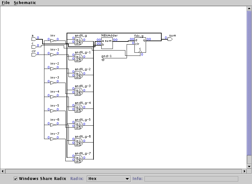
public class accum extends Logic {
public static CellInterface[] cell_interface = {
in("clr", 1),
in("a", 8),
out("sum", 8),
};
public accum(Node parent, Wire clr, Wire a, Wire sum) {
super(parent);
connect("clr", clr);
connect("a", a);
connect("sum", sum);
// An accumulator is simply an adder,
// a register bank,
// and an AND gate that forces zero on the feedback path
// Here is the output wire for the adder
Wire addOut = wire(8, "addOut");
// Here is the feedback from the register to add back in
Wire feedback = wire(8, "feedback");
// Create an instance of our adder
new NBitAdder(this, a, feedback, addOut);
// Build the actual accumulator register out of 8 flip flops
// The reg_o() call works for any width wires
reg_o(addOut, sum);
// To clear the adder, take the outputs of the register and
// pass them through an AND gate. When "clr" is high, make
// the AND gate outputs be zero.
// We will use a for-loop to build these
for (int i=0;i<8;i++)
and_o(not(clr), sum.gw(i), feedback.gw(i));
}
}
After reading through this, you hopefully realized that it is a simple thing to make this accumulator parameterized just like the adder. Here is the modified design:
import byucc.jhdl.base.*;
import byucc.jhdl.Logic.*;

public class NBitAccum extends Logic {
  public static CellInterface[] cell_interface = {
    in("clr", 1),
    in("a", "WID"),
    out("sum", "WID"),
    param("WID", INTEGER),
  };

  public NBitAccum(Node parent, Wire clr, Wire a, Wire sum) {
    super(parent);

    int wid = a.getWidth();
    bind("WID", wid);
    connect("clr", clr);
    connect("a", a);
    connect("sum", sum);

    // An NBitAccumulator is simply an adder,
    //   a register bank,
    //   and an AND gate that forces zero on the feedback path

    // Here is the output wire for the adder
    Wire addOut = wire(wid, "addOut");

    // Here is the feedback from the register to add back in
    Wire feedback = wire(wid, "feedback");

    // Create an instance of our adder
    new NBitAdder(this, a, feedback, addOut);

    // Build the actual NBitAccumulator register out of flip flops
    // The reg_o() call works for any width wires
    reg_o(addOut, sum);


    // To clear the adder, take the outputs of the register and
    //   pass them through an AND gate.  When "clr" is high, make
    //   the AND gate outputs be zero.
    // We will use a for loop to build these
    for (int i=0;i < wid;i++)
      and_o(not(clr), sum.gw(i), feedback.gw(i));

  }
}
A careful comparison of the two files will show that only minimal differences exist. Thus, in general, it is not much harder to make a design parameterized in JHDL than to make one with hard-coded wire widths.
In addition, the JHDL User's
Manual covers the operation of the range of tools associated with
the JHDL system for design simulation and netlisting.
| | JHDL Home Page | Configurable Computing Lab | Prev (Overview) | Next (User's Manual) | |
![]()
JHDL 0.3.45
Copyright (c) 1998-2003 Brigham Young University. All rights reserved.
Last updated on 11 May 2006